


_(dingoo_misc).PNG)

 Рейтинг: 4.8/5.0 (1834 проголосовавших)
Категория: Windows: Диагностика, тесты
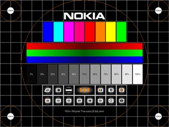
Nokia Monitor Test – большой набор тестов, необходимых для проверки работы TFT LCD, ЭЛТ мониторов.
Утилита содержит необходимые шаблоны для проверки геометрии, сведения, разрешения, муара, контрастности, яркости, фокусировки, читабельности текста, цветопередачи. Это отличный способ проверить понравившийся монитор перед покупкой.
Nokia Monitor Test предназначена для проверки качества компьютерных мониторов по различным критериям. Nokia Monitor Test не требует установки и полностью бесплатна. Программа проводит тестирование по таким критериям как: резкость, конвергенция или искажение геометрии.
Nokia Monitor Test is a freeware utility by Nokia that will guide you through testing and adjusting any monitor for an optimum display. There are test patterns for Geometry, Convergence, Resolution, Moir. Brightness, Contrast, Focus, Readability, Color and Screen Regulation. You put up the test pattern and then make the adjustments to your monitor.
There is also an excellent help file that explains all the technical terms and procedures necessary to understand how to correctly set up and adjust your monitor. You might also want to check out DisplayMate Technologies. This company writes the software that all the computer magazines use to test and compare monitors. They also write video diagnostic software for professionals. There is a wealth of information on these pages with everything from what to look for when you buy a new monitor, how to care for it, and how you should adjust it.
Nokia Monitor Test runs under all versions of Windows and can be used on any computer display. There is nothing to install. Simply extract the zip file into a directory of your choice and a Nokia Test directory will be created. You can run the program directly from the directory or make a shortcut to Ntest.exe and run it from where ever you wish.
Nokia Monitor Test may not be the newest or the most advanced display diagnostic software available but it is easy to use … and you can’t beat the price!
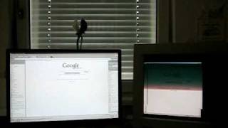
Видео Nokia Monitor Test:


Тестирование монитора бывает полезным непосредственно при его покупке, чтобы убедиться в качестве изделия. Можно использовать программу и для анализа имеющегося в наличии оборудования, чтобы правильно произвести его оптимальную настройку.
Интерфейс программы прост и понятен интуитивно. Но если у пользователя возникают вопросы по ходу выполнения тестов, он всегда может решить их с помощью встроенной справки. Помощь к программе написана на русском языке и содержит подробное описание имеющихся в программе шаблонов.
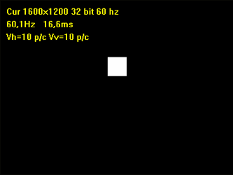
В начальном окне теста можно выбрать один из предлагаемых двенадцати тестов. Для проверки дискретности и линейности матрицы можно использовать тест градиента цвета или ступенчатого градиента. Для проверки синхронности роста яркости составляющих цветов применяется тест с цветными клиньями.
Для проверки интерполяции разрешений, которые могут быть установлены, используется тест окружностей, а также набор дополнительных тестов. Для проведения этого анализа на главной странице программы необходимо выбрать необходимое разрешение.
Можно проверить читаемость шрифтов на мониторе, а также использовать тестовую сетку для того, чтобы проверить разборчивость деталей.
В то время, когда работают тестовые шаблоны, есть возможность изменения яркости. Возможно также перемещение между шаблонами внутри одного теста.
После выполнения тестирования пользователю при необходимости даются рекомендации по оптимальной настройке используемого монитора.
Эта программа может использоваться также и для тестирования TFT телевизоров, но у них должна иметься возможность подключения к компьютеру.
Бесплатные аналоги: Nokia Monitor, IsMyLcdOK, LCD monitor test.
Платформа: Windows.
Размер: 30 Kb.
Лицензия: бесплатная.
Сайт программы: http://tireal.com/index.php?page=rtft.
Программы для тестирования монитора неизменно привлекают внимание пользователей ПК. Пожалуй, среди всех информационно-диагностических утилит они являются наиболее популярными. А все оттого, что каждый пользователь рано или поздно озаботится покупкой нового монитора. Просто выбрать производителя и модель недостаточно. Согласно правилам, монитор при покупке необходимо придирчиво протестировать.
Для чего мы тестируем монитор
Монитор старого типа, на базе трубки ЭЛТ, воспроизводит изображение, рисуя его на поверхности стеклянной колбы с помощью электронного луча, а точнее, трех лучей для основных цветов - красного, синего и зеленого. Сложная система отклонения и фокусировки - самый важный элемент монитора, от которого всецело зависит общее качество изображения. Именно ее мы и должны тестировать при покупке монитора типа ЭЛТ. Разброс технологических параметров в данном случае неизбежен, да и процесс настройки монитора на заводе часто проводится не до конца, поэтому от экземпляра к экземпляру мониторы могут существенно отличаться по качеству.
Программы тестирования мониторов облегчают задачу проверки и настройки ЭЛТ-монитора. Специальные тестовые изображения (шаблоны) позволяют выявить такие дефекты, как отсутствие сведения лучей для разных цветов, недостаточная фокусировка и стабилизация напряжения, искажения геометрии, низкая контрастность, неравномерность свечения люминофора. Просмотрев несколько экземпляров, мы можем выбрать тот, у которого отклонения от нормы минимальны.
Самой популярной и "раскрученной" программой такого профиля, без сомнения, является "Nokia Monitor Test". Нельзя сказать, чтобы эта программа имела самый большой набор шаблонов для тестирования монитора. Однако простой и понятный интерфейс, небольшой размер и полная бесплатность сделали ее настоящим хитом. Несмотря на приличный возраст (программа разработана еще в 1995 году!), она до сих пор пользуется спросом. В 2000 году появилось обновление программы, которое, впрочем, затронуло, в основном, интерфейс.
ЖК-мониторы требуют иного подхода
Для тестирования ЖК-мониторов программы типа Nokia Monitor Test не подходят по определению. Отсутствие отклоняющей системы в принципе обесценивает добрую половину шаблонов, имеющихся у таких программ. У всех мониторов на основе ЖК-панели не может быть проблем с геометрией, сведением, стабилизацией, фокусом и т.д. И разброс параметров им, в общем-то, не свойственен, за исключением "битых" пикселов, которые до сих пор встречаются, несмотря на все усилия производителей.
И тем не менее, ЖК-мониторы тоже следует тестировать. Только не разные экземпляры, а модели различных производителей. Мониторы ЖК существенно отличаются друг от друга по таким параметрам, как углы обзора, инерционность (послесвечение и "смазывание"), натуральность цветопередачи, цветовое разрешение, яркость и контраст, равномерность подсветки. Эти параметры либо вообще не указываются в характеристиках, либо измеряются по совершенно не состоятельным методикам. Например, предельным углом обзора многие производители считают такой угол, при взгляде под которым черный и белый цвет в центре (!) экрана различаются по яркости всего в пять (!) раз. Что происходит с краями экрана и какой оттенок приобретают цвета под таким углом, их не интересует. Кроме того, данные приводятся обычно не для монитора, а для ЖК-панели, которая тестировалась на стенде еще до монтажа.
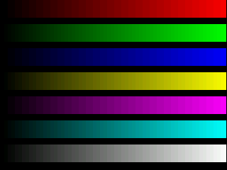
Хорошие программы для тестирования ЖК-мониторов должны позволить вам разглядеть все характерные недостатки. Их шаблоны должны создать максимально неблагоприятные условия, при которых все дефекты будут подчеркнуты. В частности, дефекты цветового разрешения и цветопередачи видны на градиентах, дефекты интерполяции "неродных" разрешений - на мелких узорах и тексте, слабая контрастность - на переходах между соседними оттенками, послесвечение - на движущихся объектах. Таких тестов в классических программах не хватает.
TFT Монитор тест
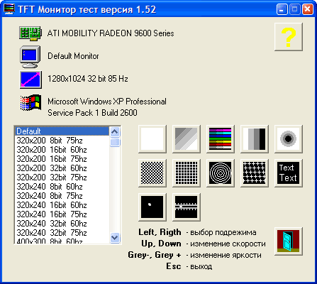
Программа с таким названием разработана отечественными программистами. В отличие от существующих аналогов, она, во-первых, совершенно бесплатна, а во-вторых, снабжена подробной справкой с описанием имеющихся шаблонов на русском языке и советами по решению типичных проблем. Программа состоит из одного файла (плюс необязательный файл справки), не требует инсталляции, в распакованном состоянии занимает всего 650 Кб - помещается на одну дискету. Налицо все признаки хорошей утилиты для тестирования.
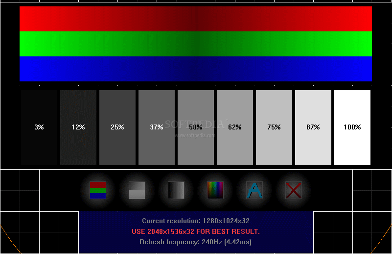
Интерфейс программы очень прост. Небольшое начальное окно позволяет выбрать разрешение (для тестирования интерполяции) либо оставить разрешение по умолчанию, а также запустить один из 12 тестов. Во время просмотра тестовых шаблонов можно регулировать яркость (очень важно для ЖК-мониторов!), перемещаться между шаблонами в пределах теста, а также переключать цвет либо направление градиента. Тестовые шаблоны позволяют проверить:
Разработчики даже попытались реализовать возможность получения количественного, а не только качественного результата. В частности, в тестах на послесвечение можно попытаться с помощью фотографии оценить длину шлейфа и по этому показателю вычислить время отклика. А в тесте на интерполяцию можно зафиксировать, на каком шаге концентрические окружности перестают сливаться. Однако это будет лишь приблизительный результат. Главное предназначение программы - провести визуальное сравнение нескольких мониторов, на которые выводятся одни и те же шаблоны одновременно.
Таким образом, программа "TFT Монитор тест" является одной из лучших в своем классе. К ее плюсам можно причислить не только большой набор статических и анимированных шаблонов, но и простоту, бесплатность, небольшие размеры дистрибутива.
Свежую версию программы "TFT Монитор тест" вы можете найти на сайте www.tfttest.fromru.com
Макс КУРМАЗ,
HW.by - Белорусский "железный" сайт
CROSS-REFERENCE TO RELATED APPLICATIONS
This application is a continuation-in-part of U.S. patent application Ser. No. 10/778,982, filed Feb. 12, 2004, and issued on Dec. 21, 2004 as U.S. Pat. No. 6,833,717. That application is entitled “Electron Beam Test System with Integrated Substrate Transfer Module.” That application is incorporated herein in its entirety by reference.
BACKGROUND OF THE INVENTION
1. Field of the Invention
Embodiments of the present invention generally relate to electron beam testing systems for semiconductor devices on substrates. More particularly, embodiments of the present invention generally relate to an improved prober for conducting a thin film transistor liquid crystal display array test on a variety of glass panel substrate designs.
2. Description of the Related Art
Active matrix liquid crystal displays (LCDs) are commonly used for applications such as computer and television monitors, cell phone displays, personal digital assistants (PDAs), and an increasing number of other devices. Generally, an active matrix LCD comprises two glass plates having a layer of liquid crystal materials sandwiched therebetween. One of the glass plates typically includes a conductive film disposed thereon. The other glass plate typically includes an array of thin film transistors (TFTs) coupled to an electrical power source. Each TFT may be switched on or off to generate an electrical field between a TFT and the conductive film. The electrical field changes the orientation of the liquid crystal material, creating a pattern on the LCD.
The demand for larger displays, increased production and lower manufacturing costs has created a need for new manufacturing systems that can accommodate larger substrate sizes. Current TFT LCD processing equipment is generally configured to accommodate substrates up to about 1.5?1.8 meters. However, processing equipment configured to accommodate substrate sizes up to and exceeding 1.9?2.2 meters is envisioned in the immediate future. Therefore, the size of the processing equipment as well as the process throughput time is a great concern to TFT LCD manufacturers, both from a financial standpoint and a design standpoint.
In order to provide quality control for thin film transistors on a large area glass substrate, it is desirable to conduct a liquid crystal display “array test.” The array test allows a TFT LCD manufacturer to monitor and correct defects in the pixels during processing. A known method of testing pixels is known as electron beam testing, or “EBT.” During testing, each TFT is positioned under an electron beam. This is accomplished by positioning a substrate on a table positioned below the beam, and moving the table in “x” and “y” directions to sequentially position each TFT on the substrate below the electron beam test device. One such device which enables flat panel display fabricators to test devices formed on flat panels is a PUMA™ electron beam tester available from AKT, Inc. a division of Applied Materials, Inc. located in Santa Clara, Calif.
In order for the LCD array test to be conducted, a “prober” is used. A typical prober consists of a frame that usually covers the entire substrate under investigation. The frame has a plurality of pogo pins thereon at locations that match the contact pads of the substrate. Electrical connection to the pogo pins is accomplished by fine wire connections to an electronics driver board. The board is usually software controlled.
In operation, the substrate is raised into contact with the prober. More specifically, the contact pads of the substrate are placed into contact with the pogo pins of the prober. The contact pads, in turn, are in electrical communication with a pre-defined set of the thin film transistors, or “pixels.” An electrical current is delivered through the pogo pins and to the contact pads. The current travels to and electrically excites the corresponding pixels. An electron beam senses voltages in the excited pixels in order to confirm operability of the various thin film transistors on the substrate.
In the past, each prober has been custom made for a particular display layout design. This means that each semiconductor device and substrate layout has required a different prober having the matching configuration for the device array. The result is that the purchaser of semiconductor fabrication machinery must also purchase a compatible prober in order to test the fabricated pixels. Moreover, the customer may desire to purchase more than one prober to serve as a backup or to simultaneously test multiple substrates.
Modification of an individual prober for a new device layout is expensive. Therefore, it is desirable to provide a prober that is configurable to match a new device layout.
SUMMARY OF THE INVENTION
The present invention generally provides an improved prober for an electronic devices test system. The prober operates to test electronic devices such as pixels on a substrate. The prober is “configurable,” meaning that it can be adapted for different device layouts and substrate sizes. In one embodiment, the prober includes a frame. The frame receives at least one adjustable prober bar having a first end and a second end. A frame connection mechanism is provided that allows for attachment of the prober bar to the frame at selected points along the frame. The prober also includes a plurality of electrical contact pins, or “pogo pins,” along the prober bar. The pogo pins place selected electronic devices on the substrate in electrical communication with a system controller during testing.
Typically, the prober will be used to test devices on a glass substrate. Preferably, each of the electronic devices is a thin film transistor. Typically, the glass substrate and the frame are each rectangular or square. In this way, “x” and “y” axes are defined by the frame. In one aspect, the at least one prober bar is placed on the frame along the “y” direction.
In one arrangement, the frame has four sides representing two opposing sides. In addition, the frame connection mechanism may define a plurality of holes along an inner surface of the four sides of the frame for receiving the first and second ends of the prober bars, respectively. In one embodiment, each prober bar includes an end cap at each of the first and second ends, with each end cap configured to be attached to selected holes of the frame connection mechanism.
In one arrangement, the prober bars are “y” bars, and the configurable prober further includes at least one “x” prober bar. The “x” bar is attached along the “y” axis of the frame orthogonal to the “y” axis. A first end of the “x” prober bar is releasably connected to the frame, and a second end of the “x” prober bar is releasably connected to one of the at least one “y” prober bars. In this arrangement, each of the “y” prober bars may have a bar connection mechanism that allows for ready relocation of the at least one “x” prober bar to the “y” prober bar at selected points along the “y” prober bar.
BRIEF DESCRIPTION OF THE DRAWINGS
So that the manner in which the above recited features of the present invention can be understood in detail, a more particular description of the invention, briefly summarized above, may be had by reference to embodiments, some of which are illustrated in the appended drawings. It is to be noted, however, that the appended drawings illustrate only typical embodiments of this invention and are therefore not to be considered limiting of its scope, for the invention may admit to other equally effective embodiments.
FIG. 1 presents a perspective view of a configurable prober, in one embodiment. The prober is part of an electronics device test system. The prober is positioned on a test system table that moves the prober in “x” and “y” directions.
FIG. 2 is a cross-sectional view of an illustrative test system table. A prober is shown schematically on the table. In addition, electron beam test columns are seen over the prober. A substrate is placed between the test table and the prober.
FIG. 3 shows the test system table of FIG. 2. In this view, the substrate has been raised into electrical contact with the prober.
FIG. 4 presents a schematic view of a configurable prober, in one embodiment. Prober bars are shown within a universal frame in the “y” direction.
FIG. 5 provides a perspective view of a prober bar oriented along the “x” axis, with an end cap at an end of the prober bar. The end cap is connected to the frame.
FIG. 6 shows the end cap of FIG. 5 exploded away from an “x” prober bar.
FIG. 7 is a partial exploded view of the prober of FIG. 4. The prober is above the base for the device testing system. Controller pads for the testing system are seen.
FIG. 8 provides a further enlarged view of the electrical connection between the prober and the base for the device testing system.
FIG. 9 presents a bottom view of an exemplary prober bar. A plurality of electrical contact pins are seen extending from the prober bar.
DETAILED DESCRIPTION
The present invention generally provides an improved prober for an electronic devices test system. For purposes of this disclosure, the term “test system” means any system that may be used to test electronic devices on a substrate. Such a test system may include optical inspection systems, electron beam test systems, systems that detect color changes, and others. The prober for the electronic devices test system is “configurable,” meaning that it can be adapted for different device layouts and substrate sizes.
FIG. 1 presents a perspective view of a configurable prober 400. in one embodiment. The prober 400 is part of an electronics device test system 100. In one embodiment, the prober 400 is part of an electron beam test system 100. though other systems could be used. The prober 400 is positioned on a test system table 110 that moves the prober 400 in at least “x” and “y” directions. In the arrangement of FIG. 1. the table 110 defines a tubular frame fabricated from stainless steel. However, the scope of the present inventions is not limited by the configuration or material of the table 110. An optional cable carrier 116 is provided external to the table 110 .
The table 110 supports various plates 120. 130. 140 that translate the prober 400 in different dimensions. The three plates 120. 130. and 140 are planar monoliths or substantially planar monoliths, and are stacked on one another. The three stacked plates are seen in cross-section in FIG. 2. which is a cross-sectional view of the illustrative test system 100 of FIG. 1 .
In one aspect, each of the three plates 120. 130. 140 is independently movable along orthogonal axes or dimensions. The first plate supports the second 130 and third 140 plates, as well as the prober 400. The first plate moves the supported second 130 and third 140 plates along a “y” axis. FIG. 1 shows bearing surfaces 122. for moving the first plate 120. The linear bearing surfaces 122 are provided in the “y” axis for the first plate 120 .
The second plate 130 supports the third plate 140. and moves the third plate 140 and prober 400 in an “x” axis. Linear bearing surfaces 132 are provided along the “x” axis for the second plate 130. The second plate 130 supports the prober 400 through a collar 135 .
Finally, the third plate 140 supports the substrate. A substrate is shown at 150 in FIGS. 1 and 2. The third plate 140 moves the substrate 150 in a “z” axis. More specifically, the third plate 140 lifts the substrate 150 into contact with pogo pins (shown at 480 in FIG. 9 ) of the prober 400 .
As indicated, a substrate 150 is shown in FIGS. 1 and 2. The illustrative substrate 150 is a large area glass substrate that contains a plurality of conductive electronic devices. An example is a plurality of thin film transistors (TFT's). It is understood that the TFT's are quite small and will not be visible in the perspective view of the test system 100 .
It is also understood that the test system 100 contains numerous other features and components. Where the test system is an electron beam test system, the system 100 may include a prober transfer assembly, a load lock chamber, a testing chamber and, optionally, a prober storage assembly, for example. The testing chamber will have electron beam columns for directing electron beams down onto the pixels under inspection. These various features are not shown in FIG. 1 ; however, electron beam columns are seen at 200 in the cross-sectional view of FIG. 2. Details of an exemplary electron beam test system containing such features are disclosed in the U.S. patent application Ser. No. 10/778,982, which was previously incorporated by reference.
Referring again to FIG. 2. a cross-sectional view of the illustrative test system 100 of FIG. 1 is presented. The test system 100 again includes a test system table 110. The table 110 supports the first plate 120. the second plate 130. and the third plate 140. The first (or lower) plate 120 and the second (or intermediate) plate 130 each move linearly along a horizontal plane, but move in a direction orthogonal to one another. In contrast, the third (or upper lift) plate 140 moves in a vertical direction or the “z” direction. Plates 120. 130 are driven by a linear motor or other actuator. Linear actuators such as linear motors or hydraulic cylinder-and-piston arrangements (not shown) may be provided for translating the plates 120. 130 .
The prober 400 is shown schematically on the table 110. supported by the plates 120. 130. 140. The plates 120. 130. 140 selectively translate the prober 400 in different dimensions. In the illustrative system 100. the prober 400 may be moved in “x”, “y” directions. Operation of the test system 100 in order to move the prober 400 is described in U.S. patent application Ser. No. 10/778,982, which is referred to and incorporated by reference herein to the extent its disclosure is not inconsistent with the present disclosure. FIG. 2 is a duplication of FIG. 5 from the pending '982 application. For this reason, discussion of the system 100 shown in FIG. 2 herein is limited.
It should be noted that the test system 100 further includes an end effector 170. A portion of the end effector is shown in cross-section in FIG. 2. The end effector 170 transfers the substrates 150 in and out of the testing chamber. In operation, the end effector 170 may be extended from the testing chamber into an adjoining chamber or system such as a load lock chamber (not shown) to load a substrate. Likewise, the end effector 170 having a substrate loaded thereon may be extended from the testing chamber into the load lock chamber to transfer the substrate 150 to the load lock chamber. A motion device, such as a linear actuator, a pneumatic cylinder, a hydraulic cylinder, a magnetic drive, or a stepper or servo motor, for example may be coupled to the end effector 170 to assist this transfer. In one aspect, the end effector 170 includes a pair of bearing blocks 172 that permit the end effector 170 to move into and out of the testing chamber. Additional features of the end effector and the transfer of substrates are provided in the '982 patent application.
The end effector 170 cooperates with the third plate 140 during substrate transfer. In this respect, the third plate contains one or more z-axis lifts 142 coupled to the plate 140. Each z-axis lift 142 is disposed within a channel 146. A bellows 148 is arranged about each lift 142 to reduce particle contamination within the testing chamber. The z-axis lift 142 moves up and down vertically and may be actuated pneumatically or electrically. The bellows 148. in turn, compress and expand in response to the movement of the corresponding lifts 142. In the view of FIG. 2. the upper lift plate 140 is in its lowered position. The substrate 150 is resting on pins 125 on the “x” plate 130 .
The illustrative test system 100 of FIG. 2 also shows electron beam testing (EBT) columns 200. In this view, one pair of columns 200 is shown. However, there will typically be two (or possibly more) pairs of EBT columns. The EBT columns 200 are disposed on an upper surface of a chamber housing 105 and are attached to the housing 105. The housing 105 provides a particle free environment and encloses the prober 400 and table 110 .
FIG. 3 shows the test system 100 of FIG. 2 in a test position. Here, the z-axis lift 142 has been actuated to raise the substrate 150. It can be seen that the substrate 150 has been raised into contact with the prober 400. More specifically, contact is made between the substrate 150 and pogo pins (not shown) on a bottom face of the prober 400 .
Moving now to FIG. 4. FIG. 4 presents a schematic view of a configurable prober 400. in one embodiment. The prober 400 has a frame 410. In the embodiment of FIG. 4. the frame 410 is a polygonal frame having four sides. In this particular arrangement, the frame is square, though other configurations may be provided such as rectangular. The frame 410 defines “x” and “y” directions or “axes.”
The prober 400 also includes one or more prober bars 420. In the view of FIG. 4. three separate prober bars 420 are shown within the frame 410 ; however, other numbers of prober bars 420 may be employed. Each of these prober bars 420 is positioned at a selected coordinate along the “x” axis, and is parallel to the “Y” axis. In this orientation, the prober bars 420 are “y” prober bars. The areas defined between the prober bars 420 form test areas 450 (seen also in FIG. 7 ).
The position of the prober bars 420 along the frame 410 may be changed. In this respect, the connection between the respective prober bars 420 and the frame 410 is releasable and relocatable. To provide for this feature, a frame connection mechanism 412 is provided that allows for ready relocation of at least one prober bar 420 to the frame 410 at a selected coordinate along the “x” or “y” axes of the frame. In one embodiment, the frame connection mechanism 412 is a plurality of through-holes placed along or formed within the inner surface of the frame 410. Exemplary through-holes are shown at 414 in the enlarged view of FIG. 5. The through-holes 414 receive end caps 440 placed at opposing ends of the prober bars 420 .
FIG. 6 provides a perspective view of an end cap 440. The end cap 440 is exploded away from an end of a prober bar 420. The end cap 440 includes one or more connecting members 444 for connecting to the frame connection mechanism 412 of the frame 410. In the end cap 440 arrangement of FIG. 6. a pair of bolts is provided as the connecting members 444. The end cap 440 also has a channel 442 for receiving a shoulder 432 on the prober bar 420. An optional bolt 446 is provided in the channel 442 of the end cap 440. The bolt 446 is configured to threadedly connect to the prober bar 420 through a threaded opening (not shown) formed on the prober bar 420 .
In order to relocate a prober bar 420 along the frame 410. the bolts 444 are backed out of the holes 414 of the frame 410. and then advanced into different holes 414 located in the frame connection mechanism 412. In this manner, the position of the prober bars 420 along the “x” axis of the frame 410 may be adjusted. This, in turn, permits the user to employ the same prober 400 for different substrate sizes and for different device configurations.
In accordance with the present invention, prober bars 420 may also be positioned in the “x” direction of the prober frame 410. meaning that the prober bars are oriented parallel to the “x” axis. FIG. 5 provides an enlarged perspective view of a prober bar 430. with an end cap 440 at an end of the prober bar 420. The end cap 440 is again connected to the frame connection mechanism 412 of the frame 410. In this orientation, the prober bar is an “x” prober bar labeled as 430. and can be moved to a different position along the “y” axis. If the dimensions of the frame 410 are different in the “x” and “y” directions, then the lengths of the “x” and “y” prober bars 430. 420 will also be different.
As an additional option, “x” prober bars 430 may be placed between “y” prober bars 420. or between a “y” prober bar 420 and the frame 410 as shown in FIG. 4. In such an arrangement (not shown), a substantially shorter “x” prober bar would be employed.
The prober 400 has a plurality of electrical connection pads 472. The pads 472 are configured to place the frame 410 in electrical communication with the testing system 100. Each of the pads 472 has a plurality of “frame” pins 470 (seen in FIG. 8 ). FIG. 7 provides a perspective view of the prober 400 of FIGS. 1 and 4 as part of the test system 100. Pads 472 are aligned with mating pads 128 on the intermediate “x” plate 130. The mating pads 128 include printed circuit boards that interface with a controller (not shown) for the testing system 100. The pads 128 receive electrical signals that come from the controller and deliver them to the connected prober electrical connection pads 472. The detachable pin 470 —pad 128 connection allows the prober 400 to be removed from the test system 100 for microscope operations and servicing. It is noted that the through-holes 414 in the frame 410 of FIG. 7 are not visible, as a cover has been temporarily placed on the prober frame 410. The cover is used during testing to shield the wires (not shown) that travel from pogo pins (shown at 480 in FIG. 9. and discussed below) to the printed circuit board 128. Without the cover, there is the potential that the E-Beam column 200 will charge up the wires. However, a cable channel for electrical connections is seen at 416 in FIG. 7 .
FIG. 8 provides a further enlarged view of the prober 400 of FIG. 7. In this view, the electrical connection between the prober frame 410 and the test system 100 is more clearly seen. In this respect, electrical frame connection pads 472 are seen aligned over test system pads 128. In addition, an alignment pin 461 is seen at a corner of the prober frame 410. The alignment pin 461 is tapered so as to be guided into a locating seat 462 provided in the upper “x” plate 130. Bolts (not seen) secure the locating seat to the upper “ye” plate 140 .
The frame electrical connection is done in such a way as to allow for a wide range of possible display layouts, such as from 25 to 1 display per sheet, and from 14? to about 50? display. More generally, the electrical connection is configurable for any display configuration that the prober frame size will accommodate.
The prober 400 also has a plurality of electrical contact pins, or “pogo” pins 480. These pogo pins 480 are placed along each of the prober bars 420. 430. FIG. 9 presents a bottom view of an exemplary prober bar 430. A plurality of electrical contact “pogo” pins 480 are seen extending from the prober bar 430. While the pogo pins 480 are shown along an “x” prober bar 430. it is understood that pogo pins would also be used for a “y” prober bar 420 .
The pogo pins 480 are configured to place the frame 410 in electrical communication with selected pixels or TFT's (or other devices) formed on the substrate 150. The pogo pins 480. in turn, are in electrical communication with the controller via the frame pins 470. As the substrate 150 is urged against the prober 400 (shown in FIG. 3 ), electrical contact between the controller and the devices on the substrate 150 is made. This allows the controller to apply a voltage to a selected pixel or to monitor each pixel for changes in attributes, such as voltage, during testing.
In one test protocol, the substrate 150 is tested by sequentially impinging at least one electron beam emitted from columns 200 (shown in FIG. 3 ) on discrete portions or pixels composing the thin film transistor matrix. After the TFT's are tested, the substrate table 110 (with supported plates 120. 130 ) moves the substrate 150 to another discrete position within the testing chamber so that another pixel on the substrate 150 surface may be tested. Additional details concerning electron beam testing are provided in the referenced '982 patent application. However, it is noted that the present disclosure provides for a selectively configurable prober 400. rather than a fixed “picture frame” prober, as disclosed in FIG. 10A of the '982 Patent Application.
While the foregoing is directed to embodiments of the present invention, other and further embodiments of the invention may be devised without departing from the basic scope thereof. For example, the frame 410 may be provided of sufficient universal size to accommodate large area glass substrates of any dimension. When a user is faced with electron beam testing of a substrate having a different dimension or a different device layout, then the user may adjust the location of the bars 420 or 430 without having to purchase an entire new prober. Where additional bars are needed, then additional bars can be purchased at an expense that is much less than an entire new prober.
In addition, an electronic devices test system 100 has been described. The test system 100 is used to test electronic devices on a substrate, such as a glass substrate 150. The test system 100 utilizes a configurable prober 400 as described above in its various embodiments. The test system 100 includes both the prober 400 and the test system table 110. In one aspect, the test system 100 further has one or more electron beam columns.
A method for testing electronic devices is also provided. The method includes the steps of providing a test system table 110 in a test system 100 ; placing a “y” table 120 on the test system table 110. the “y” table 120 being selectively movable along the test system table 110 parallel to a “y” axis; placing an “x” table 130 on the “y” table 120. the “x” table 130 being selectively movable along the “y” table 120 parallel to an “x” axis; placing a configurable prober 400 on the “x” table 130 ; and placing a substrate 150 to be tested above the “x” table 130. the substrate 150 having contact pads (not visible) and a plurality of electronic devices (also not visible) in electrical communication with selected contact pads.
The prober 400 is in accordance with the prober 400 described above, in its various embodiments. Generally, the prober 400 has a frame 410. at least one prober bar 420 or 430 having a first end and a second end, a frame connection mechanism 412 that allows for ready relocation of the at least one prober bar 420 or 430 to the frame 410 at a selected coordinate along the frame 410. and a plurality of pogo pins 480 along the at least one prober bar 420 or 430 for placing selected electronic devices in electrical communication with a system controller during testing. In one aspect, the method further includes the step of placing at least some of the plurality of pogo pins 480 in electrical communication with the contact pads.
Preferably, the method further includes the step of placing a “z” plate 140 on the “x” plate 130. In this arrangement, the substrate 150 is placed on the “z” plate 140. In one embodiment, the method further includes the step of raising the “z” plate 140 in order to raise the substrate 150 and place the pogo pins 480 in electrical communication with the contact pads. Preferably, the substrate 150 is a glass plate, and each of the electronic devices is a thin film transistor.
The scope of the inventions is determined by the claims that follow.
Для многих жидкокристаллические дисплеи (LCD) ассоциируются, прежде всего, с плоскими мониторами, "крутыми" телевизорами, ноутбуками, видеокамерами и сотовыми телефонами. Некоторые добавят сюда КПК, электронные игры, банковские автоматы. Но существует еще множество областей, где необходимы дисплеи с высокой яркостью, прочной конструкцией, работающие в широком диапазоне температур.
Плоские дисплеи нашли применение там, где критичными параметрами являются минимальные энергопотребление, вес и габариты. Машиностроение, автомобильная промышленность, железнодорожный транспорт, морские буровые установки, горное оборудование, наружные торговые точки, авиационная электроника, морской флот, специальные транспортные средства, системы безопасности, медицинское оборудование, вооружение — вот далеко не полный перечень применений жидкокристаллических дисплеев.
Постоянное развитие технологий в этой области позволило снизить стоимость производства LCD до такого уровня, при котором произошел качественный переход: дорогая экзотика стала обыденным явлением. Важным фактором быстрого распространения ЖК-дисплеев в промышленности стала и простота применения.
В этой статье рассматриваются основные параметры различные типов жидкокристаллических дисплеев, что позволит сделать осознанный и правильный выбор LCD для каждого конкретного применения (метод "побольше и подешевше" практически всегда оказывается слишком дорогим).
Все многообразие ЖК-дисплеев можно разделить на несколько типов в зависимости от технологии производства, конструкции, оптических и электрических характеристик.
Технология
В настоящее время при производстве LCD применяются две технологии (рис.1): пассивная матрица (PMLCD-STN) и активная матрица (AMLCD).
Технологии MIM-LCD и Diode-LCD не получили широкого распространения и поэтому не будем на них тратить время.
Рис. 1. Виды технологий жидкокристаллических дисплеев
STN (Super Twisted Nematic)— матрица, состоящая из ЖК-элементов с изменяемой прозрачностью.
TFT (Thin Film Transistor)— активная матрица, в которой каждый пиксел управляется отдельным транзистором.
По сравнению с пассивной матрицей, TFT LCD имеет более высокую контрастность, насыщенность, меньшее время переключения (нет "хвостов" у движущихся объектов).
Управление яркостью в жидкокристаллическом дисплее основано на поляризации света (курс общей физики): свет поляризуется, проходя через поляризационный фильтр (с определенным углом поляризации). При этом наблюдатель видит только снижение яркости света (почти в 2 раза). Если за этим фильтром поставить еще один такой фильтр, то свет будет полностью поглощаться (угол поляризации второго фильтра перпендикулярен углу поляризации первого) или полностью проходить (углы поляризации совпадают). При плавном изменении угла поляризации второго фильтра интенсивность проходящего света будет также плавно изменяться.
Принцип действия и "бутербродная" структура всех TFT LCD примерно одинакова (рис. 2). Свет от лампы подсветки (неоновая или светодиоды) проходит через первый поляризатор и попадает в слой жидких кристаллов, управляемых тонкопленочным транзистором (TFT). Транзистор создает электрическое поле, которое формирует ориентацию жидких кристаллов. Пройдя такую структуру, свет меняет свою поляризацию и будет — или полностью поглощен вторым поляризационным фильтром (черный экран), или не будет поглощаться (белый), или поглощение будет частичным (цвета спектра). Цвет изображения определяют цветовые фильтры (аналогично электронно-лучевым трубкам, каждый пиксел матрицы состоит из трех субпикселов — красного, зеленого и голубого).
Рис. 2. Структура TFT LCD
Пиксел TFT
Цветные фильтры для красного, зелёного и синего цветов интегрированы в стеклянную основу и расположены близко друг к другу. Это может быть вертикальная полоса, мозаичная структура или дельта-структура (рис. 3). Каждый пиксел (точка) состоит из трёх ячеек указанных цветов (субпикселей). Это означает, что при разрешении m x n активная матрица содержит 3m x n транзисторов и субпикселов. Шаг пиксела (с тремя субпикселами) для 15.1" TFT ЖК-дисплея (1024 x 768 точек) составляет примерно 0.30 мм, а для 18.1" (1280 x 1024 точки)— 0.28 мм. TFT LCD имеют физическое ограничение, которое определяется максимальной площадью экрана. Не ждите разрешения 1280 x 1024 при диагонали 15" и шаге точки 0.297 мм.
Рис. 3. Структура цветного фильтра
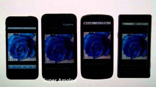
На близком расстоянии точки явственно различимы, но это не беда: при формировании цвета используется свойство человеческого глаза смешивать цвета при угле зрения менее 0,03°. На расстоянии 40 см от ЖК-дисплея при шаге между субпикселами 0,1 мм угол зрения составит 0,014° (цвет каждого субпиксела различит только человек с орлиным зрением).
Типы ЖК-дисплеев
TN (Twist Nematic) TFT или TN+Film TFT — первая технология, появившаяся на рынке ЖК-дисплеев, основное достоинство которой& — дешевизна. Недостатки: черный цвет больше похож на темно-серый, что приводит к низкой контрастности изображения, "мертвые" пиксели (при выходе из строя транзистора) очень яркие и заметные.
IPS (In-Pane Switching) (Hitachi) или Super Fine TFT (NEC, 1995 год). Характеризуется наибольшим углом обзора и высокой точностью цветопередачи. Угол обзора расширен до 170°, остальные функции — как у TN+Film (время отклика порядка 25мс), практически идеальный черный цвет. Преимущества: хорошая контрастность, "мертвый" пиксель — черный.
Super IPS (Hitachi), Advansed SFT (производитель — NEC). Достоинства: яркое контрастное изображение, искажения цвета почти незаметны, увеличены углы обзора (до 170° по вертикали и по горизонтали) и обеспечена исключительная четкость.
UA-IPS (Ultra Advanced IPS), UA-SFT (Ultra Advanced SFT) (NEC). Время реакции достаточно для обеспечения минимальных искажений цвета при просмотре экрана под разными углами, повышенная прозрачность панели и расширение цветовой гаммы при достаточно высоком уровне яркости.
MVA (Multi-Domain Vertical Alignment) (Fujitsu).Основное преимущество — наименьшее время реакции и высокая контрастность. Главный недостаток — высокая стоимость.
PVA (Patterned Vertical Alignment) (Samsung). Микроструктурное вертикальное размещение ЖК.
Конструкция
Конструкция жидкокристаллического дисплея определяется расположением слоев в "бутерброде" (включая и светопроводящий слой) и имеет наибольшее значение для качества изображения на экране (в любых условиях: от темного помещения до работы при солнечном свете). В настоящее время используются три основных типа цветных LCD:
Компромиссной разновидностью пропускающего типа дисплея для работы, как в помещении, так и при внешнем освещении, является полупрозрачный (transflective) тип конструкции.
Пропускающий тип дисплея (transmissive). В этом типе конструкции свет поступает сквозь жидкокристаллическую панель с задней стороны (подсветка) (рис. 4).По этой технологии сделаны большинство ЖК-дисплеев, используемых в ноутбуках и карманных компьютерах. Transmissive LCD имеет высокое качество изображения в помещении и низкое (черный экран) при солнечном свете, т.к. отраженные от поверхности экрана солнечные лучи полностью подавляют свет, излучаемый подсветкой. Эта проблема решается (в настоящее время) двумя способами: увеличением яркости задней подсветки и уменьшением количества отраженного солнечного света.
Рис. 4. Конструкция жидкокристаллического дисплея пропускающего типа
Для работы при дневном освещении в тени необходима лампа подсветки, обеспечивающая 500 кд/м2, при прямом солнечном свете — 1000 кд/м 2. Яркости в 300 кд/м 2 можно добиться путем предельного увеличения яркости одной лампы CCFL (Cold Cathode Fluorescent Lamp) или добавлением второй лампы, расположенной напротив. Модели жидкокристаллических дисплеев с повышенной яркостью используют от 8 до 16 ламп. Однако увеличение яркости подсветки увеличивает расход энергии батарей (одна лампа подсветки потребляет около 30% энергии, используемой устройством). Следовательно, экраны с повышенной яркостью можно использовать только при наличии внешнего источника питания.
Уменьшение количества отраженного света достигается нанесением антиотражающего покрытия на один или несколько слоев дисплея, заменой стандартного поляризационного слоя на минимально отражающий, добавлением пленок, повышающих яркость и, таким образом, увеличивающих эффективность источника света. В ЖК-дисплеях Fujitsu преобразователь заполняется жидкостью с коэффициентом рефракции, равным коэффициенту рефракции сенсорной панели, что значительно сокращает количество отраженного света (но сильно сказывается на стоимости).
Полупрозрачный тип дисплея (transflective) похож на пропускающий, но у него между слоем жидких кристаллов и подсветкой имеется т. н. частично отражающий слой (рис.5). Он может быть или частично серебряным, или полностью зеркальным со множеством маленьких отверстий. Когда такой экран используется в помещении, он работает аналогично transmissive LCD, в котором часть освещения поглощается отражающим слоем. При дневном освещении солнечный свет отражается от зеркального слоя и освещает слой ЖК, при этом свет проходит жидкие кристаллы дважды (внутрь, а затем наружу). Как следствие, качество изображения при дневном освещении ниже, чем при искусственном освещении в помещении, когда свет проходит LCD один раз.
Рис. 5. Конструкция жидкокристаллического дисплея полупрозрачного типа
Баланс между качеством изображения в помещении и при дневном освещении достигается подбором характеристик пропускающего и отражающего слоев.
Отражающий тип дисплея (reflective) имеет полностью отражающий зеркальный слой. Все освещение (солнечный свет или свет передней подсветки) (рис. 6), проходит сквозь ЖКИ, отражается от зеркального слоя и снова проходит сквозь ЖКИ. В этом случае качество изображения у дисплеев отражающего типа ниже, чем у полупропускающего (так как в обоих случаях используются сходные технологии). В помещении передняя подсветка не так эффективна, как задняя, и, соответственно, качество изображения — ниже.
Рис. 6. Конструкция жидкокристаллического дисплея отражающего типа
Основные параметры жидкокристаллических панелей
Разрешение. Цифровая панель, число пикселей в которой строго соответствует номинальному разрешению, должна корректно и быстро масштабировать изображение. Простой способ проверки качества масштабирования — изменение разрешения (на экране текст, написанный мелким шрифтом). По контурам букв легко заметить качество интерполяции. Качественный алгоритм дает ровные, но немного размытые буквы, тогда как быстрая целочисленная интерполяция обязательно вносит искажения. Быстродействие — второй параметр разрешения (для масштабирования одного кадра требуется время на интерполяцию).
Мертвые пиксели. На плоской панели могут не работать несколько пикселей (они всегда одного цвета), которые появляются в процессе производства и восстановлению не подлежат.
Стандарт ISO 13406-2 определяет предельные значения количества дефектных пикселов на миллион. В соответствии с таблицей ЖК-панели делятся на 4 класса.